Below are few questions which you can try over LTSPICE yourself and understand the different design concpets. It will help you in VLSI Industry, the real simulation based concepts.
Please try to solve these questions yourself.
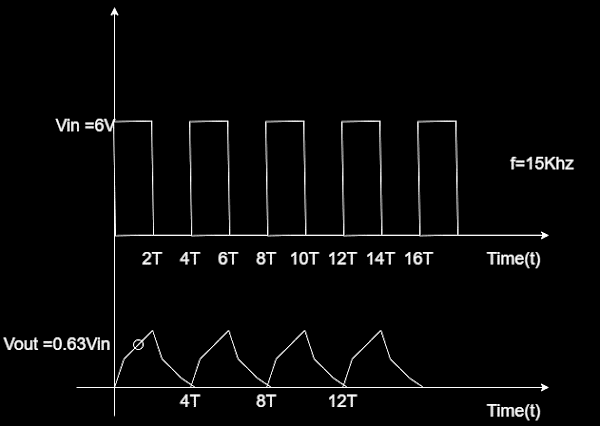
Q1) Design the circuit which is provided with the input Vin as shown in left figure and output is obtained as Vout as shown in the right figure
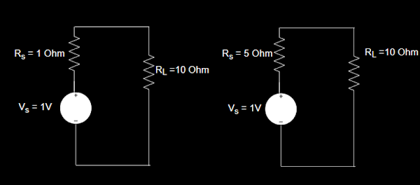
Q2) For the circuit shown below which one is better Explain and support your answer with LTSPICE Simulation
Q3) For the given netlist generate the schematic on LTSPICE. What kind of analysis is being done here
VIN 1 7 AC 0V
IST 0 10 AC 1MA
VX 10 6 DC 0V
VDD 8 0 15V
RS 1 2 250
C1 2 3 IUF
R1 8 3 1.4MEG
R2 3 0 1MEG
RD 8 4 15K
RS1 5 9 100
RS2 9 0 15K
CS 9 0 20UF
C2 4 6 0.1UF
R3 6 7 15K
R4 7 0 5K
M1 4 3 5 5 MQ
.MODEL MQ NMOS (VTO=1 KP =6.5E-3 CBD=5PF
+RG =0 RDS =1MEG CGSO=1PF CGDO=1PF CGBO=1PF)
.AC DEC 10 10HZ 10MEGHZ
.PROBE
.END
Q4) Design a circuit for the given input and output waveform given below and after designing it draw the schematic on LTSPICE and verify that the circuit indeed generate the waveform given in here
Q5) Explain what is wrong in the Model statements given below
1)
.MODEL MQ NMOS (VTO=1 KP =6.5E-3 CBD=5PF
+RG =0 RDS =1MEG CGSO=1PF CGDO=1PF CGBO=1PF)
R1 4 3 5 5 MQ
2)
.MODEL QNP NPN (BF =50 RB=70 RC =40 TF =0.1NS TR =10NS VJC=0.85)
M1 4 3 2 QNP
3)
.MODEL DIODE D (RS =40 TT =0.1NS)
Q1 4 5 DIODE
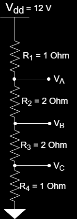
Q6) For the Circuit shown below:
- Shown the voltage across the Resistor R3 and R4
- Find the Voltage VA ,VB,VC
- Also Justify the value using LTSPICE Simulation
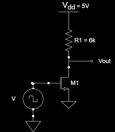
Q7) For the circuit shown below write the netlist also you need to include the model used for MOSFET and Resistor
-Prepared By Niti Gupta
(Director of eLearning and university Program)
(VLSI Expert Private Limited)
-Supervised By Puneet Mittal
(Founder & Director)
(VLSI Expert Private Limited)
(Director of eLearning and university Program)
(VLSI Expert Private Limited)
-Supervised By Puneet Mittal
(Founder & Director)
(VLSI Expert Private Limited)


No comments:
Post a Comment