Friday, December 24, 2021

TCL Practice Task S2_1 (Scripting Language)


While working on industry grade EDA tools, it is important to understand the working of commands. However most important are switches used along with the commands. These switches are designed in such a way that it acquire sufficient information from the end user (user that is using the command). As a end user you can control the command also or say you can instruct the program to execute the command in a specific manner.
For Example There is a program that can extract 10 different informations from a file but may be as a user you don't want all those information at the same time. If you want that program should give you only 5 informations, than obviously you have instruct the program. A good program is the program which give flexiblity to the end user to instruct the program (even though that's your program but end user think that they are controling the program :) )

Both the above mentioned things can be easily done with the help of switches. There are 2 type of switches.
  • Optional Switch
    • It's user dependent
    • If user define/uses these switches while runing/executing the program, respective program of task is going to perform else no need to perform task
  • Mandatory Switch
    • User has to provide the value of this else program is not going to work - or program will give you an error
So, I am back here to help you in developing that skill along with automation which will create a background of understanding that how industry tools works.

This is the first program of Second series of TCL Scripting language. If you have done all 4 task of Series 1, It's good but in case you missed that - Complete them first (even before starting this program).  TCL Practice Task 1TCL Practice Task 2, TCL Practice Task 3TCL Practice Task 4,


PART 1 of S2_1

Step 1: Create a input file as mentioned below.    

##################################################################


Startpoint: DFFPOSX1_3 (rising edge-triggered flip-flop clocked by clk)
Endpoint: out1 (output port clocked by clk)
Path Group: reg-to-out
Path Type: max

Delay      Time          Description
---------------------------------------------------------------
0.00          0.00          clock clk (rise edge)
1.23          1.23          clock network delay (prop)
0.16          1.39  ^     DFFPOSX1_3/CLK (DFFPOSX1)
0.27          1.66  v     DFFPOSX1_3/Q (DFFPOSX1)
0.08          1.74  v     BUFX2_1/Y (BUFX2)
0.13          1.87  v     out1 (out)
                1.87 data arrival time

1.00      1.00      clock clk (rise edge)
1.43      2.43      clock network delay (prop)
-0.25     2.18      Uncertainty
0.54      2.72      clock reconvergence pessimism
-2.50     0.22      output external delay
            0.22      data required time
---------------------------------------------------------------
           0.22      data required time
            -1.87      data arrival time
---------------------------------------------------------------
    slack     -1.65      (VIOLATED)

Startpoint: DFFPOSX1_3 (rising edge-triggered flip-flop clocked by clk)
Endpoint: out1 (output port clocked by clk)
Path Group: reg-to-out
Path Type: max

Delay      Time      Description
---------------------------------------------------------------
0.00          0.00      clock clk (rise edge)
1.23         1.23        clock network delay (prop)
0.16         1.39  ^     DFFPOSX1_3/CLK (DFFPOSX1)
0.27         1.66  v     DFFPOSX1_3/Q (DFFPOSX1)
0.08         1.74  v    BUFX2_1/Y (BUFX2)
0.13         1.87  v    out1 (out)
                1.87    data arrival time

1.00          1.00      clock clk (rise edge)
1.43          2.43      clock network delay (prop)
-0.25         2.18     Uncertainty
0.54          2.72     clock reconvergence pessimism
-2.50         0.22     output external delay
                 0.22      data required time
---------------------------------------------------------------
                0.22    data required time
                -1.87   data arrival time
---------------------------------------------------------------
slack     -1.43      (VIOLATED)

##################################################################

Step 2 : You have to create a command line script cum procedure, which will take the Step 1 as a input file with a switch; and other user defined switch which will output the certain values. It should be like “report_parameter.tcl -input report.txt -dat -drt -slack -cppr -skew -path_group” 

(Note: I am not specifying the switch name - you can choose yourself. Use a Switch --help which user can use to find out all the switches). 

Step 3 : Output should be dumped into a csv file (Comma separated value file). This is very common file in Industry and whenever you are going to open this file using excel or libreoffice (in linux). Please find the csv file snapshot.

Parameters, Report 
slack,-1.65
ext_delay,3.00
uncertainty,0.25
cppr,0.54
data path delay,1.87
Skew,0.20


PART 2 of S2_1


Repeat all the steps with the help of attached file - which is bigger in size and as per Industry requirement.

STEP 1 Full report_file

I am sure this article will help you to prepare for TCL scripting. I have few more such programs which I will try to capture later sometime.


-By Rajat Bansal
(Btech-EC:- 2019 Passout)
https://www.linkedin.com/in/rajat-bansal-3400009b/


-Supervised By Puneet Mittal
(Founder & Director)
(VLSI Expert Private Limited)

Wednesday, December 15, 2021

LTSPICE Based Self-Practice Questions

We have seen a lot of students facing problems while working on several basic concepts. To understand those concepts, it's very much required to do some testing and simulation and assess yourself how much you are able to grasp the concepts.

Below are few questions which you can try over LTSPICE yourself and understand the different design concpets. It will help you in VLSI Industry, the real simulation based concepts.

Please try to solve these questions yourself.

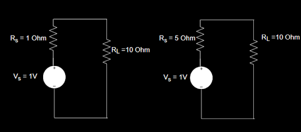
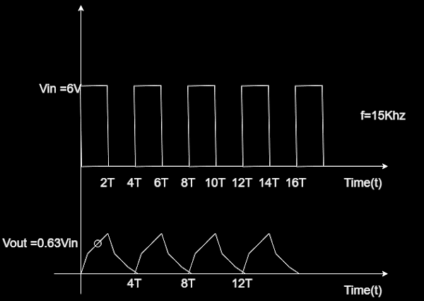
Q1) Design the circuit which is provided with the input Vin as shown in left figure and output is obtained as Vout as shown in the right figure


Q2) For the circuit shown below which one is better Explain and support your answer with LTSPICE Simulation


Q3) For the given netlist generate the schematic on LTSPICE. What kind of analysis is being done here

VIN 1 7 AC 0V
IST 0 10 AC 1MA
VX   10 6 DC 0V
VDD 8 0   15V
RS    1  2    250
C1    2  3    IUF
R1    8  3    1.4MEG
R2    3  0   1MEG
RD    8  4     15K
RS1   5  9     100
RS2   9  0      15K
CS     9  0       20UF
C2    4   6       0.1UF
R3    6   7      15K
R4    7   0      5K
M1  4   3    5   5 MQ
.MODEL MQ NMOS (VTO=1 KP =6.5E-3  CBD=5PF
+RG =0 RDS =1MEG CGSO=1PF CGDO=1PF CGBO=1PF)
.AC DEC 10 10HZ 10MEGHZ
.PROBE
.END


Q4) Design a circuit for the given input and output waveform given below and after designing it draw the schematic on LTSPICE and verify that the circuit indeed generate the waveform given in here


Q5) Explain what is wrong in the Model statements given below

1)
.MODEL MQ NMOS (VTO=1 KP =6.5E-3 CBD=5PF
+RG =0 RDS =1MEG CGSO=1PF CGDO=1PF CGBO=1PF)
R1    4  3  5  5   MQ

2)
.MODEL QNP NPN (BF =50 RB=70 RC =40 TF =0.1NS TR =10NS VJC=0.85)
M1    4  3  2  QNP

3)
.MODEL DIODE D (RS =40 TT =0.1NS)
Q1    4  5  DIODE

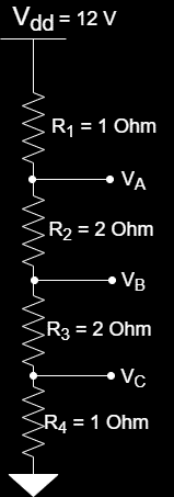
Q6) For the Circuit shown below:
  1. Shown the voltage across the Resistor R3 and R4
  2. Find the Voltage VA ,VB,VC
  3. Also Justify the value using LTSPICE Simulation


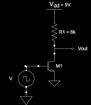
Q7) For the circuit shown below write the netlist also you need to include the model used for MOSFET and Resistor


-Prepared By Niti Gupta
(Director of eLearning and university Program)
(VLSI Expert Private Limited)

-Supervised By Puneet Mittal
(Founder & Director)
(VLSI Expert Private Limited)

Sunday, June 6, 2021

Latch Based Timing Analysis - Part 2 (Capture and Launch Edges)

In the last article (Latch Based Timing Analysis - Part 1) of this series, we have discussed general differences and correlation between Latch and Flipflop from Timing analysis point of view. We have discussed, how in case of Latches, Edges are also important and what's the significance of those edges.
Just to summarize or say refresh your memory, below are few points along with respective figure.


  1. Latches start sampling data from the Start Edge respective to Enable level. Means, if Latch is Positive level - respective Start edge is Rising edge (as showing in figure)
  2. Latches continue sampling data at Enable Levels (either Positive or Negative)
  3. Latches stop sampling data at the End Edge respective to Enable Level. If Latch is Positive level - respective stop edge is Falling edge (as showing in figure)
  4. In case of 2 Latch based circuit (one is Launch Latch and other as Capture Latch), if we want to Launch data at one level (assume at X1 - as in fig) from one Latch and capture the data at other Level (assume at X2 - as in fig), It's important to understand first/last edge of Launch & Capture latch(Please refer last article for detail)

If above concepts are clear, lets try to understand the circuit & respective waveform based on 3 latches. Because that's very important to understand this concepts.

In Above figure, there are 3 Latches (L1, L2 & L3) connected back to back. Lets assume L1 launches the data at the rising edge. There are 2 different paths between the latches and that's the reason it's reaching at L2 at 2 different time. Blue one is with respect to shortest path and Red one is with respect to longest path. If you have noticed that both the datas are reaching after 10ns (sometime after L2 latch become enable) but as Latch is level triggered and L2 is enabled at this time. So, L2 capture the data at D pin and launches it to next timing path at the same moment (not considering the delay of latch in this example).

Important point to understand at this stage - data reaching at L2 at 2 different time (depending on data path between L1 and L2), the moment data reaches at L2, it will automatically launched by L2 (because L2 is enable/transparent at that time). So, now you can see that launching time/point for data is different by L2.

If combinational circuit between L2 and L3 also have smallest and longest path - means data again have 2 combinations
  • Red data with shortest path
  • Red data with longest path
  • Blue data with shortest path
  • Blue data with longest path
but for simplicity purpose, we have only represented 2 set of data - Red data with Longest path and Blue data with shortest path. You can draw picture with other 2 combination and try to understand the yourself. Consider this an exercise for you :).

Data launches by L2, reaches at 2 different time at L3 (as shown in figure). Since, L3 is enabled at that time, it will again launch it at the same time. If you have noticed the Time line - Data launched by L1 at 0ns can easily launched by L3 (even in worst case) at 25ns.

Now, lets try to undestand what's going to happen if same combinational circuit is present between the Flipflop.

Flip-flop F1 is going to launch the data at 0ns, because of presence of smallest and longest path, data is reaching at F2 at 2 different time and after 10ns. Since, F2 is a positive edge triggered flip-flop & data were not present in either of case before 10ns, data has to wait for next positive edge at F2.

Next positive edge is going to be at 20ns and irrespective of data travelling any path (smallest path or longest path) between F1 and F2, F2 is going to capture it at 20ns and launch the data for next Timing path between F2 and F3.

Again data travel through shortest and longest data path and reaches at F3 at 2 different time. As per the figure, again you can see data is not reaching before 30ns (which is the next rising edge point at F3), so data has to wait for next rising edge which is at 40ns. So, F3 is going to capture the data and launches it at 40ns.

So, In summary, I can say - Data launched by FF1 at 0ns, launched by FF3 (even in worst case) at 40ns.

This much understanding is sufficient for this Article. At least, now you can see how much time we are saving just replacing the Flip-flop with latches and how our circuit become fast by using latches. But on the other side, complexity also increases. In case of Flipflop, it's very simple that Lauch and Capture edge is going to be at edges and we have to make sure that data reaches before capture edges but in case of Latch, a lot of othe concepts comes into the analysis. and Don't worry - we are going to discuss those concepts in this series of Articles :).

Stay Tune for next article.

Monday, May 31, 2021

High Level Synthesis - Part 1 - Introduction

High Level Synthesis is the technology of 21st Centuary. Lot of industry is working in this area and unfortunatly you will find very less information abou this. We as in VLSI Expert, always try to fill such gaps. These series of articles are going to give you an indept knowledge from basic to advance. Author of this article is Mr. Rishabh Jain (Senior Member Technical Staff, Mentor Graphics Pvt. Ltd.). On our request, he agree to share his experience. This is the first article of couple of more which are in Pipeline.

Table of Contents


Proclaiming the Requirement
Diving into the History
Defining the rescuer
Understanding the Use Case
References

Proclaiming the Requirement

As a hardware designer, what do you think is the most brainstorming step when you try to convert the provided specification to the corresponding implementation? Is it HDL modelling you are going to choose? Or maybe the technology library you are going to use? Or perhaps the best clock frequency possible which gives best performance, area and power?
The aim is to make a design with the best suitable architecture to suffice the specification requirement.
Let’s consider the following design:

module top(clk,arst,din,dout);

input clk;
input arst;
input [31:0] in;
output reg [31:0] out;

always@(posedge clk or posedge arst)
  begin
  if(arst == 1'b1)
     out <= 32'b0;
  else
     out <= in;
  end

endmodule

What you see above is a Verilog based design of a D-Flip-Flop
For experts in the domain it is pretty evident that precisely it is a D-Flip-Flop with Asynchronous reset functionality.

For the amateurs, let me explain a bit here –
INPUT pins are clk clock pin, arst an asynchronous reset pin and in a 32-bit input data bus.
OUTPUT pin is out a 32-bit output data bus.
At every positive clock edge or at positive reset edge, we transmit value of in to out data bus if arst is 0 else we transmit a 32-bit 0 value to out data bus.

The design above represents an active high reset functionality. Consider a scenario where you wish to reuse the above DFF design with active low reset or maybe a DFF with synchronous reset. You would have to re-code the HDL code as the different requirement of architecture arises but with same functionality.
To overcome the problem, let’s consider the same design with High Level Synthesis (HLS):

void top( int in, int& out)
{
   out = in;
}

Yep! That’s pretty much it. Roughly a few lines code in C++ that too without the restrictions of providing reset or clock. That can be easily added later during the synthesis process. The key here is to understand the focus functionality and providing the freedom to the designer in terms of experimenting with multiple architecture types to fulfil the requirements.

But now you might be asking what exactly this HLS is? What happened to traditional HDL methodologies for designing? Are there any additional advantages to what explained above? Where is the definition of input and output or the data bus width in the HLS design mentioned above?

Let’s see the answers to all of these questions.

Diving into the History

In VLSI design process, synthesis has been a significant process in the initial stages of the ASIC and FPGA design flows. Synthesis can be simply defined as the process of transforming your design from a higher level of abstraction to a lower level of abstraction.

In terms of hardware description languages (HDLs), we define synthesis as converting HDL model of hardware (higher abstraction) to the corresponding gate-level implementation of the hardware (Lower abstraction).

The process of designing hardware has changed a lot over the years from handwritten netlist design to CADs to HDLs and is still evolving for the betterment and ease of designing with the increase in complexity. Below table shows the growth of design complexity in terms of number of transistors involved over the past few decades.
With increasing design complexity, hardware designing process involved usage of HDLs like Verilog and VHDL which indeed brought a revolution in the VLSI industry having the key advantages as follows:
  • Easy to express large designs and flexibility
  • Abstraction hides the complexity of the design
  • Time to market is reduced.
  • Optimization is easier with trade off capabilities (area vs speed)
The most widely used design methodology involves behavioral modelling in HDLs which helps the designer to focus on the functionality of the specification rather than the resultant hardware model of it.

As the algorithms being used, especially when dealing large and complex Machine Learning algorithms evolved, HDL modelling methodology started to seem highly unlikely to fulfil designer’s requirement. Consider the following limitation of using HDLs:
  • Hard to design complex algorithmic designs like Computer Vision, Image Processing etc.
  • Faster time to market with good quality of results is very challenging.
  • High verification cost & debug time.
  • Flexibility for handling frequent changes in specifications is not present.
  • With change in technology library, design has to be modified, e.g. FPGA to ASIC.
The above-mentioned drawbacks highlight the need of some methodology which focuses on functionality and provides the freedom to design large algorithms without stressing upon the architectural needs. Thus we advocate and highlight the point that these problems can be easily taken to consideration with High Level Synthesis. Let me define the same in the next section.

Defining the rescuer

As we have discussed so far, there is a need for a methodology which can be used for designing complex algorithms and focuses on functionality more than the timing aspect of it. The process of high-level synthesis seems to resolve this issue.

High Level Synthesis (HLS) can be defined as the automated designing process that transforms the behavioral or functional description of the design into a digital hardware implementation. Now some may argue the point that high-level synthesis could be interchangeably used with the term behavioral synthesis. When we define the different kinds of modelling pertaining to HDLs, behavioral modelling and synthesis seemed to fit the definition of HLS. But the only problem is the lack of methodology in this process.

To begin with, the design entry language was unfamiliar as not all the designers were comfortable with behavioral Verilog or VHDL. Moreover, the problem of using the synthesizable construct like “always block” or “(@posedge clk)” was hindering the designer’s focus on algorithmic designing.
In order to establish a methodology, high level languages were introduced in the process of hardware designing. Thus, HLS primarily started the use of C, C++ and SystemC as the designing languages which in turn made writing complex algorithms easier.
Therefore, we define High Level Synthesis as the process which takes C/C++/SystemC (High level language) as an input or algorithmic description of the design and produces the result as a corresponding FSM and data path as an output which is further processed into the formation of the hardware description language (HDL) based RTL netlist.

Please note that while designing with HLS, functionality or the algorithmic behavior of the design is the priority and not the timing aspect or the architecture of it.
So now that we have understood what HLS is, let me explain the power of it using an example in the next section.

Understanding the Use Case

In the first section while explaining the requirement and making the case for HLS, I represented the ease of designing with the help of a DFF with asynchronous reset where no clock or reset has been provided at this stage in the HLS design.

The port width is simply defined using C++ native “int” datatype which is by default 32-bit wide and “&” operator is used to represent the direction of the registered output port. Additionally, interface protocol details automatically gets included by the HLS tool as shown below:

Let us see another example of designing a 32-bit 4 Input adder with HLS.

void acc (int din[4], int &dout)
{
   int acc=0;

   for (int i=0; i<4; i++)
   {
    acc += din[i];
   }

   dout = acc;
}

The design has 4 32-bit inputs din[0] down to din[3]. The output of the design, as stated using a “&” operator, is dout which is a 32-bit wide data bus.
So far we have only specified the functionality as the sum of all the 4 inputs to be transmitted to the output data bus.

Please not that no information with respect to architecture has been provided. We can easily achieve multiple hardware implementations using the same design.
For instance, we can have fully parallel registered output implementation like:
The above implementation is not optimized in terms of resources being used as we can see 3 adders in the resultant hardware.

For achieving minimum area we can have different constraints and force the tool to use a single adder resource. The resultant would be something like:
Similarly, a fully pipelined version of the adder can also be achieved by providing a different set of architectural constraints.
Now imagine having to do the same with RTL designing. Designer would probably be writing different Verilog RTL implementation code for all the 3 adder architectures discussed above. This is the power and flexibility of the HLS.
From the above example, following advantages of HLS can be easily observed:
  1. Higher level of abstraction, therefore, focus on algorithms.
  2. Trade Off between Area and timing is flexible as per requirement.
  3. Reusability is much easier.
  4. Technology library independent designing
  5. Late spec changes can be incorporated with least possible efforts.
Now you probably be asking that how to provide the clock in D-FlipFlop design explained above? How about the reset as well? Where do we mention the synchronous or asynchronous nature of it? Also, where can we give architectural constraints for having a specific kind of 32-bit Adder as per the requirement?

Embrace yourself and stay tuned for the upcoming series of articles where I’ll explain the answers to all the above questions and highlight the power of HLS designing methodology.


References:

https://en.wikipedia.org/wiki/High-level_synthesis
https://semiengineering.com/whats-the-real-benefit-of-high-level-synthesis/
https://www.cse.usf.edu/~haozheng/teach/cda4253/doc/hls/hls_bluebook_uv.pdf

Author:

Rishabh Jain Senior Member Technical Staff, Mentor Graphics Pvt. Ltd.

Wednesday, April 28, 2021

Static Timing Analysis based on Operating Conditions

Understanding of operating condition-based analysis is very important, if you really want to be expert in Static Timing Analysis. PVT (like Process, Voltage and Temperature) corners, Interconnect corners, Design Corners are all inter-related and these numbers are increases day by day. These are few topics where people have a lot of confusion (and there was time even I was at the same stage). Still sometime I become confused. But still, I am trying to capture my understanding here as per my experience & try to simplify these concepts as much as possible. In this series of Articles, I am going to discuss about this in very detail. I will try my best to cover as much as possible in a simple language.

Let’s start with the Type of Analysis based on Operating Conditions & then we will go one step down to understand concepts in great detail. I am sure all of you will Like this series of Articles.

Type of Analysis based on Operating Conditions

When we have studied (in college days) about the Semiconductor devices & different equations & respective parameter, we have noticed that these parameters have dependency on Environment Temperature or Fabrication Process or Voltages. There are few constants which we have used in the equations & if you will try to find out the concepts behind the value of those constants, you will see that there is certain assumption made and if you try to remove those assumption – equation become more complex. We are going to discuss all these in this series of Articles by like I said one by one.

In lot of books/manuals/readme/flow/methodology/articles, you will see people usually talk about 3 type of Analysis mode for STA (Static Timing Analysis) on the basis of Operating conditions. Those 3 analysis modes are…
Single Operating condition Analysis mode - means it’s going to use single set of Delay values for whole circuit based on Process, Voltage and Temperature. For example, reading only 1 .lib file for setup and Hold analysis.

BC_WC Operating condition Analysis mode – it’s known as Best case Worst Case operating mode. It means we are going to use 2 extreme set of delay values simultaneously based on respective Process, Temperature & Voltage. For example, you are going to use 2 .lib files for Setup and Hold Analysis. For Setup check, we use Max & Min delay values from 1 .lib file and for Hold Check - Max & Min delay values from another .lib file.

OCV Operating condition Analysis mode – OCV stands to On-Chip-Variation. We will discuss this in detail later. In this mode, we use 2 set of delay values at the same time for Timing Analysis. For example – For Setup analysis, Max delay for Launch Clock path & Data path; Min delay for Capture clock path from both set of Libraries. Similarly – For Hold Analysis, Min delay for Launch Clock path & Data path; Max delay for Capture Clock path.

Note: Please read the difference between BC_WC Vs OCV mode.

I am sure, you become more confuse. No problem 😊 … Let’s take an example and try to understand this.

We have a small circuit as per below Fig; 2 set of Libraries (.lib files) example_bc.lib & example_wc.lib. For easy understanding I am using delay values directly (detailed calculation of delay value will discuss in next Article).


Combination Logic Delay as per example_bc.lib
For Falling waveform at Q1: 7ns
For Rising waveform at Q1: 5ns
Buffer delay as per example_bc.lib
Fall delay = 2ns
Rise delay = 3ns
Clock2Q delay as per example_bc.lib
0.8ns if falling waveform at Q1
1.0ns of rising waveform at Q1
Combination Logic Delay as per example_wc.lib
For Falling waveform at Q1: 10ns
For Rising waveform at Q1: 8ns
Buffer delay as per example_wc.lib
Fall delay = 3ns
Rise delay = 4ns
Clock2Q delay as per example_bc.lib
1.0ns if falling waveform at Q1
1.2ns of rising waveform at Q1

Setup Time of FF2 = 2.5ns
Hold Time of FF2 = 3ns
Clock Time Period = 10ns

Few other assumptions during the analysis:- Note:
  • I have just mentioned the delay values directly as per the circuit but actually tool is going to calculate the delay value based on Transition time and output Load. To understand that part please refer my other articles.
  • Setup and Hold Time also have dependency on type of waveform at D2 pin but right now just making it simple. 😊

Let’s try to understand how the calculation happen in all 3 Mode for Setup and hold Analysis. But before that I want you to revise the Setup and Hold Slack equation. 😊 You can also check my other article for this http://www.vlsi-expert.com/p/static-timing-analysis.html

Setup Slack = Required Time – Arrival Time
Required Time (RT)= Capture Clock Path delay (Min) + Time Period – Setup Time
Arrival Time (AT)= Launch Clock path Delay (Max) + Clock2Q Delay (max) + Datapath delay (Max)

Hold Slack = Arrival Time - Required Time
Required Time (RT) = Capture Clock Path delay (Max) + Hold Time
Arrival Time (AT) = Launch Clock path Delay (Min) + Clock2Q Delay (Min) + Datapath delay (Min)

Single Operating Mode:

As we have discussed, for such analysis we provide only one delay table for Setup ad Hold analysis. In our case we have 2 .lib files that means we can do 2 analysis.

Single Operating condition analysis using example_bc.lib
Setup Analysis:
RT = 3 x (Buffer Rise Delay) + 10ns – (Setup Time) = 3x3ns + 10ns -2.5ns = 16.5ns
AT = 3 x (Buffer Rise Delay) + Clock2Q Delay (falling waveform at Q1) + Combinational Delay (Falling waveform at Q1)
= 3x3ns + 0.8ns + 7ns = 16.8ns
Setup Slack = RT – AT = 16.5ns – 16.8ns = -0.3ns (Violation)

Question
  • I have picked Rise Buffer delay in both cases, Why?
  • I have used Clock2Q delay is for falling waveform at Q1 even though Rising waveform Delay at Q1 is more then falling waveform delay at Q1, Why?
Hold Analysis:
RT = 3 x (Buffer Rise Delay) + (Hold Time) = 3x3ns + 3ns = 12ns
AT = 3 x (Buffer Rise Delay) + Clock2Q Delay (Rising waveform at Q1) + Combinational Delay (Rising waveform at Q1)
= 3x3ns + 1.0ns + 5ns = 15ns
Hold Slack = AT – RT = 15ns – 12ns = 3ns (No Violation)

Single Operating condition analysis using example_wc.lib
Setup Analysis:
RT = 3 x (Buffer Rise Delay) + 10ns – (Setup time) = 3x4ns + 10ns -2.5ns = 19.5ns
AT = 3 x (Buffer Rise Delay) + Clock2Q Delay (falling waveform at Q1) + Combinational Delay (Falling waveform at Q1)
= 3x4ns + 1.0ns + 10ns = 23ns
Setup Slack = RT – AT = 19.5ns – 23ns = -3.5ns (Violation)

Hold Analysis:
RT = 3 x (Buffer Rise Delay) + (Hold time) = 3x4ns + 3ns = 15ns
AT = 3 x (Buffer Rise Delay) + Clock2Q Delay (Rising waveform at Q1) + Combinational Delay (Rising waveform at Q1)
= 3x4ns + 1.2ns + 8ns = 21.2ns
Hold Slack = AT – RT = 21.2ns – 15ns = 6.2ns (No Violation)

Single Mode Analysis Summary
Analysis Type Using Library example_bc.lib Using Library example_wc.lib
Setup Slack -0.3ns -3.5ns
Hold Slack 3ns 6.2ns

So, in this mode you have to do 2 separate analysis. Tool will read only 1 .lib at a time and perform analysis as per that.

There may be couple of questions in your mind in terms of values while doing setup and hold analysis. I say either wait for some time or revise your concepts once again. 😊

Let’s Jump to the second Mode of analysis

Min_Max (Bc_Wc) Operating Mode:

In this mode we have to provide or say define 2 set of libraries inside the tool – one as Best-case Library and other as worst-case library. Like we already have 2 libraries – so just define it.
Best_Case_Library = example_bc.lib
Worst_case_Libary = example_wc.lib

You can ask me on what basis we are going to define it – means in our case, library name itself has bc/wc, so is it the criteria? What if library name doesn’t have such nomenclature? Simple Answer from my side it – you have to get an IDEA for this. If you define these libraries randomly, your analysis is not going to be a good analysis. Generally, in most of the companies there is a separate Team which do all these experiments and update you which is Best/worst library, so you can use that as your reference OR if you want to know yourself – This series of Articles is for you. 😊 We are going to discuss all these in detail in coming articles. But for now, just use above case and try to understand how it will impact the analysis.

Setup Analysis:
For Setup, we (or say tool) are going to use only worst-case library defined by you i.e. example_wc.lib

RT = 3 x (Buffer Rise Delay) + 10ns – (Setup time) = 3x4ns + 10ns -2.5ns = 19.5ns
AT = 3 x (Buffer Rise Delay) + Clock2Q Delay (falling waveform at Q1) + Combinational Delay (Falling waveform at Q1)
= 3x4ns + 1.0ns + 10ns = 23ns
Setup Slack = RT – AT = 19.5ns – 23ns = -3.5ns (Violation)

Hold Analysis:
For Hold, we (or say tool) are going to use only best-case library defined by you i.e. example_bc.lib

RT = 3 x (Buffer Rise Delay) + (Hold Time) = 3x3ns + 3ns = 12ns
AT = 3 x (Buffer Rise Delay) + Clock2Q Delay (Rising waveform at Q1) + Combinational Delay (Rising waveform at Q1)
= 3x3ns + 1.0ns + 5ns = 15ns
Hold Slack = AT – RT = 15ns – 12ns = 3ns (No Violation)

BC_WC Mode Analysis Summary:
Analysis Type Best Case Library = example_bc.lib
Worst Case Library = example_wc.lib
Setup Slack -3.5ns
Hold Slack 3ns

If you will compare BC/WC operating mode analysis with Single Mode Analysis, you may realize that both are same as such only difference is – we are doing less no. of analysis in BC/WC mode. Yes, you are right and don’t think we are losing anything. For Setup, we want to make sure that even in worst case – my design should work – so for that we are doing worst case analysis, For Hold, we want to make sure that even in Best case scenario my design should work and that’s the reason we did best case analysis. As such, rest 2 analysis are not required. So, we are saving a lot of Run Time also. Saving a lot of Tool runtime + Memory + CPU uses + Human analysis time. That’s the importance of BC_WC_Operating_mode Analysis.

Now, Let’s try to understand the 3rd Mode of Analysis.

On-Chip-Variation Analysis Mode:

There are lot of concepts in this mode but we are going to discuss only basic one right now. Later in series, we will extend this mode and discuss in detail. So, as we have discussed that in this mode also we are going to use 2 set of libraries and we have to define the worst and best case libraries as we have done in case of BC_WC_Operating Mode but difference is in the way we are performing Setup and Hold analysis.
If you will see the Setup and Hold Slack equations – (Again pasting here)

Setup Slack = Required Time – Arrival Time
Required Time (RT)= Capture Clock Path delay (Min) + Time Period – Setup Time
Arrival Time (AT)= Launch Clock path Delay (Max) + Clock2Q Delay (max) + Datapath delay (Max)

Hold Slack = Arrival Time - Required Time
Required Time (RT) = Capture Clock Path delay (Max) + Hold Time
Arrival Time (AT) = Launch Clock path Delay (Min) + Clock2Q Delay (Min) + Datapath delay (Min)

We have talked about the min delay for capture clock path and max delay in launch clock path in case of setup but in above 2 analysis mode (Single Mode analysis & BC_WC_mode), we are not using different set of delays for different paths. Yes, you got the point correctly – in this mode we will do analysis keeping this in considering.
Best_Case_Library = example_bc.lib
Worst_case_Libary = example_wc.lib

Setup Analysis:
For Setup, we (or say tool) are going to use worst-case means max delay for Arrival path (Arrival Time) from the library defined as worst_case library (i.e. example_wc.lib ) and best-case means min delay for Required Path (Required Time) from the library defined as best_case library (i.e. example_bc.lib )

RT = 3 x (Buffer Rise Delay from Library example_bc.lib) + 10ns – (Setup time)
= 3x3ns + 10ns -2.5ns = 16.5ns
AT = 3 x (Buffer Rise Delay from Library example_wc.lib) + Clock2Q Delay (falling waveform at Q1, as per library example_wc.lib) + Combinational Delay (Falling waveform at Q1, as per library example_wc.lib)
= 3x4ns + 1.0ns + 10ns = 23ns
Setup Slack = RT – AT = 16.5ns – 23ns = -6.5ns (Violation)

Hold Analysis:
For Hold, we (or say tool) are going to use bst-case means min delay for Arrival path (Arrival Time) from the library defined as best_case library (i.e. example_bc.lib ) and worst-case means max delay for Required Path (Required Time) from the library defined as worst_case library (i.e. example_wc.lib )

RT = 3 x (Buffer Rise Delay from Library example_wc.lib) + (Hold Time) = 3x4ns + 3ns = 15ns
AT = 3 x (Buffer Rise Delay from Library example_bc.lib) + Clock2Q Delay (Rising waveform at Q1, as per Library example_bc.lib) + Combinational Delay (Rising waveform at Q1, as per Library example_bc.lib)
= 3x3ns + 1.0ns + 5ns = 15ns
Hold Slack = AT – RT = 15ns – 15ns = 0ns (No Violation)

OCV Mode Analysis Summary:
Analysis Type Best Case Library = example_bc.lib
Worst Case Library = example_wc.lib
Setup Slack -6.5ns
Hold Slack 0ns

Now, lets compare all the 3 mode and see what’s our finding and I am sure you can yourself decide the advantage of each mode.
Remember:
Best_Case_Library = example_bc.lib
Worst_case_Libary = example_wc.lib


Analysis Type Single Mode BC_WC Mode OCV Mode
BC LibraryWC library
Setup Slack -0.3ns -3.5ns -3.5ns -6.5ns
Hold Slack 3ns 6.2ns 3ns 0ns

Note:
  • OCV mode is more closure toward the real scenario –
    • If you fix setup slack in this mode – it will fix in other mode of analysis also.
    • If there is no Hold Violation in this mode – it will not be in other 2 also

Still, Lot of questions are there related to these 3 modes, Wait for next Article in next week.