Monday, October 30, 2017

Technology File: Modelling of Dielectric Layer

Background of Types of Dielectric layer


Dielectric layers are of 2 types.
  1. Planar Dielectric
  2. Conformal Dielectric
Note: We have already discussed about the conformal dielectric in detail. You can review once again (Click here).

Below figures can help you to refresh your memories about Planar and Conformal dielectric.

Planar Dielectric:

All Dielectric in the below figure (D1 to D7) are Planar dielectric.


Conformal Dielectric:

Different type of Conformal dielectric structures are shown in below figure. There are certain parameters which helps to identify any conformal dielectric like Side thickness, Bottom thickness or Top thickness.


Modelling of Dielectric in Technology File


Modelling of Dielectric layer in technology file vary as per extraction software or you can say that as per EDA vendor. Different EDA vendor uses different ways to represents this as per their requirement. Even if I know their syntax, I can't write here. :) But what I am going to do - explain everything in more easy language. :) Once you start working, you can check their manual and try to map my syntax with their syntax. :)

To represent a Planar Dielectric (Non-Conformal) we need to have following basic information.

(Parameter Name : my_nomenclature )
Dielectric constant : di_constant
Thickness : thickness
Height from the Substrate : height
Name of Dielectric : DIELECTRIC
Type of Dielectric : conformal=false

To represent a Conformal Dielectric we need to have following extra information.

(Parameter Name : my_nomenclature )
Side Thickness : S_thickness
Bottom Thickness : B_thickness
Top Thickness : T_thickness
Type of Dielectric : conformal=true
Parent Layer : p_layer (This is the layer around which dielectric is present. It can be a conductor like Poly, Metal1 or may be any other Dielectric also. In above figure, M1 is the Parent layer).

Planar Dielectric


Modelling in Technology file:

DIELECTRIC DEL2
  di_constant = 4.8
  thickness = 2.7
  height = 4.1
  conformal = false

DIELECTRIC DEL3
  di_constant = 2.8
  thickness = 0.3
  height = 6.8
  conformal = false

Conformal Dielectric

There are different scenarios which need to understand. These scenarios are same as we have discussed in the article of Conformal Dielectric (It will help you to map easily)

Scenario 1:


Modelling in Technology file:

DIELECTRIC DEL_M1a
  conformal = true
  T_thickness = 0.2
  S_thickness = 0.2
  B_thickness = 0
  di_constant = 3.8
  thickness = 0
  height = 4.1
  p_layer = M1

DIELECTRIC DEL_M1b
  conformal = true
  T_thickness = 0
  S_thickness = 0.2
  B_thickness = 0.2
  di_constant = 3.8
  thickness = 0
  height = 4.1
  p_layer = M1

Scenario 2:


Modelling in Technology file:

DIELECTRIC DEL_a
  conformal = true
  T_thickness = 0.2
  S_thickness = 0
  B_thickness = 0
  di_constant = 3.8
  thickness = 0
  height = 4.1
  p_layer = M1

DIELECTRIC DEL_b
  conformal = true
  T_thickness = 0
  S_thickness = 0.2
  B_thickness = 0
  di_constant = 3.8
  thickness = 0
  height = 4.1
  p_layer = M1

DIELECTRIC DEL_c
  conformal = true
  T_thickness = 0
  S_thickness = 0
  B_thickness = 0.2
  di_constant = 3.8
  thickness = 0
  height = 4.1
  p_layer = M1

Scenario 3:


Representation of DEL_a1, DEL_a2 and DEL_a3 in Technology file:

DIELECTRIC DEL_a1
  conformal = true
  T_thickness = 0.2
  S_thickness = 0
  B_thickness = 0
  di_constant = 3.8
  thickness = 0
  height = 4.1
  p_layer = M1

DIELECTRIC DEL_a2
  conformal = true
  T_thickness = 0.15
  S_thickness = 0
  B_thickness = 0
  di_constant = 2.8
  thickness = 0
  height = 4.1
  p_layer = DEL_a1

DIELECTRIC DEL_a3
  conformal = true
  T_thickness = 0.15
  S_thickness = 0
  B_thickness = 0
  di_constant = 1.8
  thickness = 0
  height = 4.1
  p_layer = DEL_a2

Remember: In above representation, for DEL_a2, p_layer is previous dielectric (i.e DEL_a1). It's because this dielectric has parent layer DEL_a1. It's deposited on the top of DEL_a1. Top thickness also measured with respect to DEL_a1.
Note: you might be thinking why Height parameter is same in all 3 cases. It depends on EDA vendor, how they want to represent the height of Conformal layer. Here I am assuming that my tool is going to automatically measure actual height with the help of provided data. :)

Representation of DEL_b1 and DEL_b2 in Technology file:

DIELECTRIC DEL_b1
  conformal = true
  T_thickness = 0
  S_thickness = 0.2
  B_thickness = 0
  di_constant = 3.8
  thickness = 0
  height = 4.1
  p_layer = M1

DIELECTRIC DEL_b2
  conformal = true
  T_thickness = 0
  S_thickness = 0.15
  B_thickness = 0
  di_constant = 2.8
  thickness = 0
  height = 4.1
  p_layer = DEL_b1

Similarly, Representation of DEL_c1 and DEL_c2 in Technology file:

DIELECTRIC DEL_c1
  conformal = true
  T_thickness = 0
  S_thickness = 0
  B_thickness = 0.2
  di_constant = 3.8
  thickness = 0
  height = 4.1
  p_layer = M1

DIELECTRIC DEL_c2
  conformal = true
  T_thickness = 0
  S_thickness = 0
  B_thickness = 0.15
  di_constant = 2.8
  thickness = 0
  height = 4.1
  p_layer = DEL_c1

Scenario 4:


Modelling in Technology file:

DIELECTRIC DEL2
  conformal = true
T_thickness = 0.1
  S_thickness = 0.2
  B_thickness = 0.0
  di_constant = 2.8
thickness = 0.4
  height = 4.1
  p_layer = M1

DEL2 is a conformal dielectric & the reason behind this is - It has a Side Thickness and Top thickness parameter. But you may be thinking that it looks like a planar at all other places, it's shape is similar to non-conformal dielectric. I can understand your confusion. Actually, you are right that at certain places it's conformal and at some places it's non-conformal.
In the representation of all conformal layer, you may have noticed that thickness parameter is 0. It's because they dnt have any thickness as such (I am not talking about top thickness. That's a different parameter). In this case, this thickness parameter is non-zero like in case of Planar dielectric.

At the end, I just wanted to highlight once again that different EDA vendors have different syntax and different way to represent dielectric layers in technology file. Above representation is just for your understanding purpose, it's not specific to any company.

Friday, October 27, 2017

Metal Layer Stack (Nomenclature) Part 2

In the last part we have discussed about the Metal Stack. The way foundry provide data, different restrictions and available options. Now it's time to understand the very next step - how to communicate the complex Metal Stack information across the design team or groups or companies. For this Foundry also provide Nomenclature of metal stack.

If you remember in the last article we have discussed that there are different metal wires like Mx, My, Mz, Mr , Mu, etc (in XYZ Foundry). Below diagram can help you to remind this very well.


Now, lets suppose you want to use Stack type 7 and same you want to communicate to other user, then there is a standard way for this. (You might be thinking that I will communicate directly that you are referring Stack type 7. But if we do this - every time user has to refer this table to understand different metal layer optons. :) ).

If you will check closely the Stack Type 7, you will find below information.
  • There are Total 6 metal layers.
  • Metal 1 is of M1 type.
  • Metal 2, 3, 4 are of Mx type. Means next 3 Metal layers (After M1) are of Mx type.
  • Metal 5 is of My type. Means next 1 metal layer (after Mx) is of is of My type.
  • Metal 6 is of Mz type. Means next 1 metal layer (after My) is of is of Mz type.

Now, if I combine all this information and write something like this.

M1_3Mx_My_Mz : 1 (M1 Type) + 3 (Mx type) + 1 (My Type) + 1 (Mz Type) = 6 Metal layer.

Between 2 metal layers (e.g M1 and M2) - we will use VIA as per upper metal layer type (e.g Vx type)
The way I have defined the sequence also help to understand the sequence of Metal layer.

Any one can now interpret that :
Metal 1 = M1
Metal 2 = Mx1 (Mx Type)
Metal 3 = Mx2 (Mx Type)
Metal 4 = Mx3 (Mx Type)
Metal 5 = My1 (My Type)
Metal 6 = Mz1 (Mz Type)

VIA 1 = Vx1 (Vx type)
VIA 2 = Vx1 (Vx type)
VIA 3 = Vx1 (Vx type)
VIA 4 = Vx1 (Vy type)
VIA 5 = Vx1 (Vz type)
Remember, number of VIAs are always 1 less then the number of Metal layers. :)

Different companies uses different way to understand this. Like following are few examples.
  1. M1_3Mx_My_Mz : 1 (M1 Type) + 3 (Mx type) + 1 (My Type) + 1 (Mz Type) = 6 Metal layer.
  2. 3Mx_My_Mz : 1 (M1 Type) + 3 (Mx type) + 1 (My Type) + 1 (Mz Type) = 6 Metal layer.
  3. 3MxMyMz : 1 (M1 Type) + 3 (Mx type) + 1 (My Type) + 1 (Mz Type) = 6 Metal layer.
  4. 6M_3MxMyMz : 1 (M1 Type) + 3 (Mx type) + 1 (My Type) + 1 (Mz Type) = 6 Metal layer.
  5. 1P6M_3MxMyMz : 1 (M1 Type) + 3 (Mx type) + 1 (My Type) + 1 (Mz Type) = 6 Metal layer.

Note:
  • In the 2nd, 3rd, 4th and 5th option, First Metal layer M1 is considered by default.
  • In the 4th option, It was mentioned explicitly that stack has 6 metal layer (6M).
  • In the 5th option, It was mentioned explicitly that stack has 1 Poly layer (1P) and 6 metal layer (6M).

For the above figure, I have added all the nomenclature as per 5th option. Also for your easiness, I have mentioned Stack name at the Top and Bottom (both places same information). I am sure, after this there will be no confusion. :)


In the last, I just wanted to highlight that above nomenclature and metal stack options is for 1 foundry. But different Foundries may have different ways to provide and representation their information. With in the companies or group or team, they can also decide their own way to represent Metal Stack but when they communicate with outside world, either they have to use certain standard or they have to provide details of their nomenclature (which is very common).

Monday, October 23, 2017

Metal Layer Stack (Metallization Option) Part 1


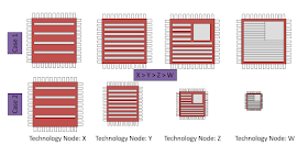
There are different metal layers which we uses in our design. As we move down the technology node number of standard cells increases or you can say that number of connections increases drastically. As all of us know that these connection are made of Metal wire, it means number of metal wires increases. Below figure help you to understand the scenario.

Case1 : I didn't decrease the size of the chip (despite change in the no of standard cells per unit area) as we go down the technology node. You can see that number of metal wires increases. Silicon utilization improves with improved routability. But these numbers (standard cell) increases 4 times (per node if we are decreases the size by 1/2, overall area decreases by 1/2*1/2=1/4). With available options of metal wire in higher node, it's difficult to route the same design in lower technology node. And that's the reason as we go down number of metal wires increases (vertically also).

Case 2: This is the real scenario. As Technology node decreases, no of standard cells increases and also chip size decreases. So you can imagine how difficult it is to route the design with a single metal wire or say on a single level. That's the reason we have multiple levels of metal wires. These levels are in vertical direction. As we go down the technology node, these levels increases. So you can say that down the technology node, size of the chip decreases in one dimension (in 2D) but increases in other dimension (vertically). :) :)

Technology Node Vs Routing Complexity

To take care about the above options, foundry provides different option of metal in every technology node. These options are based on metal width, space, thickness or sometime other parameters. (You will get more clarity as we discuss more).

Type of Metal Wire


On the basis of Metal wire parameter or say property, foundry divide or say categorize different metals. These metal wire are named differently to distinguish from each other. Let's assume XYZ foundry have nomenclature of Mx, My, Mz, Mr. Different technology node will have different options. For example.

In Technology node X.

Mx:   First Inter-layer Metal:   Min_width = 0.1um & Min_space = 0.1um.
My:   Second Inter-layer Metal:   Min_width = 0.4um & min_space = 0.4um.

In Technology node Y.

Mx:   First Inter-layer Metal:   Min_width = 0.08um & Min_space = 0.08um.
My:   Second Inter-layer Metal:   Min_width = 0.18um & min_space = 0.18um.
Mz:   Top Metal layer:       Min_width = 0.4um & min_space = 0.4um
Mr:   Top Metal layer:       Min_width = 0.5um & min_space = 0.5um

In Technology node Z.

Mx:   First Inter-layer Metal:   Min_width = 0.05um & Min_space = 0.05um.
Mya:   Second Inter-layer Metal:   Min_width = 0.12um & min_space = 0.12um & thickness = 2800A
Myb:   Top metal layer:   Min_width = 0.12um & min_space = 0.12um & thickness = 3200A
Mz:   Top Metal layer:       Min_width = 0.4um & min_space = 0.4um
Mr:   Top Metal layer:       Min_width = 0.5um & min_space = 0.5um

Note: These min_width and min_spacing numbers are not related to any technology node. I just picked these randomly to help you to understand how different metal wires are categorized.

As we go down these available options increases. Like Mx, My, Mz, Mu, Mr, Mw and so on. For exact numbers of metal and their property plz refer foundry provided documents.

Foundry also recommend based on the uses of metal wire. Like few metal wire options with a relaxed pitch (minimum_width + minimum_spacing = Pitch) for power, clock, busses and other important signal distribution. Tighter pitched options for general signal routing. You can also see (In Technology Node Z) that Mya and Myb are also 2 different type of metal wire because their Thickness values are different (even though their min_width and min_spacing are same). So you can understand that as per the uses, foundry provides a lot of options. Now it's upto designer how to use those options.

Foundry provide this (above) information in several ways so that user can understand it very clearly. One thing I want to highlight here that user have flexibility to choose metal layers but out of available options. Stay tune to understand this point.

Cross-section diagram of a Metal Stack:


First try to understand below pic :)


This is basically a cross-section of different metal wire after the fabrication. In the sense, how different metals are placed and how they are connected. Sometime lot more details can be provided along with this pictorial view like min_width and min_spacing of every metal wire, name of the dielectric, thickness of metal wire and dielectric. It varies from foundry to foundry & process to process.

Another representation of cross-section of Metal Stack (Source: VLSI Research INC - Downloaded from Internet)


Here you can see, they have explained from real fabrication point of view and also explained what are different components of first metal film stack, second metal film stack and so-on as per their process.

Note: Above cross-section foundry can provide for maximum available Metal stack. Now if you are confused what is the meaning of "available" metal stack (refer below pic)

Tabular diagram of Metal Stack:


Basically it's metallization option available or say provided by the foundry. They can provide this in the table form to make things crystal clear. Cross-section diagram can help you but drawing the cross-section of each and every stack is not possible. So they created table something like this (below).

Note: I have only created a very small subset of actual table but it is sufficient to understand foundry data.


I have only captured 21 stack type. There can be more also. Now let's try to understand this table more closely.
  • For 3 Metal layer - there is only 1 option available. (Stack type 1)
  • For 4 Metal layer - there is only 1 option available. (Stack type 2)
  • For 5 Metal layer - there is only 2 option available. (Stack type 3,4)
  • For 6 Metal layer - there is only 3 option available. (Stack type 5,6,7)
  • For 7 Metal layer - there is only 6 option available. (Stack type 8-13)
  • For 8 Metal layer - there is only 8 option available. (Stack type 14-21)
  • There are no other available options for any metal layer stack apart from provided in the table. Like if you need any other combinations of metals for 5 metal layer, it's not available. (Restriction provided by foundry)
  • Metal layer "Mr" can not be used in case of 3, 4, 5 &6 metal layer stack. (Restriction provided by foundry)
  • Top Metal layer can be of either Mz or Mr (for metal stack more then 6). (Restriction provided by foundry)
  • My, Mx Layer can't be Top metal layer. These are always inter-layer metal. (Restriction provided by foundry)
  • M1 is always First metal layer. (Restriction provided by foundry)
  • Sequence of Metal layer is M1 -> Mx -> My -> Mz/Mr. You can't change the sequence. (Restriction provided by foundry)

Following information can supplement above diagram (also provided by foundry) and sometime easy to understand. If you can understand this properly, you can form any stack diagram or say you can understand all available options provided by foundry.


Similar type of table can be provided for VIA also.

Now from Foundry point of view, every things looks good. But you may be thinking
  • How this information is going to use in the design?
  • How are designers going to communicate with each other about a certain metal stack?
  • Is there any standard for communication point of view with in a Design Team?
You may have lot of other questions, Lets wait for second part of this article to understand more about the Metal Layer Stacking from Designer point of view.

Sunday, October 22, 2017

Physical Design Interview Questions (Part 2)


Second part of this series. There are few sets of questions which is very common from Physical Design Interview point of view.
One of my Student shared below questions with me and as I always do - Sharing with everyone. :) He told me that he got offer from 6 service based companies after practicing only these questions. I haven't validated his statement and going with his words. :)

Note: Not mentioning the Answer of these questions right now. But I will do that later on. If anyone of you can do this for me or others (in lesser time compare to my time)- that will be great. I will explain these Answers one by one in detail fashion, so obviously it will take time. :)

Third Set of questions (Asked in third Company)
Remember- first 2 set of questions already covered in previous article.
  1. What are the inputs given to PnR / What it contained?
  2. What are things will you do in data-setup?
  3. How will you place macros?
  4. Let A, B, C, D are four macro in a block, A & B are in same hierarchy and they are communicating with each other, D is also in same hierarchy as A & B but not communicating with A & B. C is in different hierarchy but communicating with D. How will you place the macros?
  5. What are the reason behind congestion between the macros?
  6. How will you find the spacing between two macros?
  7. How will you resolve congestion inside Standard cell?
  8. What is power planning?
  9. How will you reduce IR Drop?
  10. What is CTS? How will you synthesis clock tree and what are clock tree optimization?
  11. What is pre-routing?
  12. What are the low power techniques we used for the submicron technology?
  13. In a timing check between 2 FF, hold slack is +2ns but setup is failed by -10ns. How will you resolve it?

These are few set of questions which has been asked in 3 companies (2 sets, I have already shared in previous article). I am sure - lots more can be asked. My intension to captured these questions at this place is not to provide a list of questions which can 100% help you to crack any interview but I want to show you a pattern of questions and the amount of preparation which you need to do.
Like I said in my previous article - "I am not saying that only these questions are sufficient for you to crack any PD (Physical Design) Interview, but I am 100% sure that these will help you to understand if your preparation is good enough and also provide you certain direction in your preparation."

Just wanted to share one incidence before I finish this article.
After my first article, one of my friend from VLSI Industry (working as senior PD manager) called me and asked if I am doing the right thing to captured all these questions.

His concern was - what if candidates don't have understanding about whole PD flow but they know (mug-up or remember) all these questions and answer all of them correctly. They can't survive in Industry for Long, so am I doing justification with them? :)

In reply of this - I just asked one question to him - Are you asking same set of questions everytime in a same sequence & wording? He got my message and I hope same with you all.

In case, you need my help to check whether you are ready for Interview or NOT, Please request for the MOCK Interview. We can connect and you are going to treat as Interviewee. After the MOCK interview, I will provide you detailed feedback.
Steps to request for MOCK Interview Sessions are below.
  1. Fill all details of this Form.
    Registration Form
  2. Book your 30min Slot
  3. After the Mock Interview - Get Detailed Feedback at your Mail id

BEST OF LUCK.

Sunday, October 8, 2017

Physical Design Interview Questions (Part 1)


There are few sets of questions which is very common from Physical Design Interview point of view.
One of my Student shared below questions with me and as I always do - Sharing with everyone. :)

Note: Not mentioning the Answer of these questions right now. But I will do that later on. If anyone of you can do this for me or others (in lesser time compare to my time)- that will be great. I will explain these Answers one by one in detail fashion, so obviously it will take time. :)

First Set of Questions (Asked in One Company)
  1. Draw APR Flow
  2. When we will place "Physical Only Cells"
  3. What are "Spare Cells" and why it is used?
  4. Why do you make clock as Ideal during floorplan & Placement Stage?
  5. What are the different Checks we do in the CTS stage?
  6. What if Setup is failed after manufacturing of chip?
  7. How will you fix Hold?
  8. What is the Importance of useful Skew?
  9. What are DRV Checks and why do we check that?
  10. What is the cross talk? How it will effect the performance?
  11. Cross delay or Cross talk noise is note generally. Why?
  12. A Blocks having 7 Metal layers and same block having 10 metal layer, which will function better and why?
  13. How will you define the shape of the Die?

Other set of questions (Asked in Second Company)
  1. Draw and Explain APR flow.
  2. How will you place Macro?
  3. How will you reduce congestion near I/O parts?
  4. Where will you implement partial blockage?
  5. What are checks you will do after each stage of PNR?
  6. What is Setup and Hold Time?
  7. Few problem based on Setup and Hold Calculation.
  8. What are the Timing check will you do apart from setup and hold check?
  9. What if Setup and Hold Both fails?
  10. How will you resolve Setup and Hold Issues?
  11. What are clock free targets and buffer constraints?
  12. How will you fix DRV?
  13. How will you do cloning?
  14. Which metal will you use for Power routing and Why?
  15. What are routing grids?
  16. What is Antenna Effect and how will you resolve it?
  17. What is Antenna Ratio?
  18. What is Latch up and How will you resolve it?
  19. How will you place TAP Cells and in which Stage will you place Tap cells?
  20. Why ENDCAP Cells are used ?
  21. What all Datas will be given to FAB after Tapout?
  22. Why Derates are used for Timing Calculation? Is it Good or Bad?

I was thinking to list down Companies name here but then realized what if they stop asking these questions. :) :) But Point is these questions are very much related to concepts of whole PD flow. I am not saying that only these questions are sufficient for you to crack any PD (Physical Design) Interview, but I am 100% sure that these will help you to understand if your preparation is good enough and provide you certain direction in your preparation.

In case, you need my help to check whether you are ready for Interview or NOT, Please request for the MOCK Interview. We can connect and you are going to treat as Interviewee. After the MOCK interview, I will provide you detailed feedback.
Steps to request for MOCK Interview Sessions are below.
  1. Fill all details of this Form.
    Registration Form
  2. Book your 30min Slot
  3. After the Mock Interview - Get Detailed Feedback at your Mail id

BEST OF LUCK.


Monday, October 2, 2017

Delay Interview Question (Part1)


Let's discuss the Delay concepts from Interview point of view. Several times it happen that Interviewer is going to ask certain questions and the moment you answer it - they will change the case or scenario without changing the Diagram or values. Few of the scenarios, I am going to discussing here. Remember - As a Interviewer - our intension is to check "how much you know" and "How much you can visualize from Tool perspective or real design point of view".

Example 1:


All Buffer has same (min, max) delay = (0.1ns, 0.2ns)
All NOT Gate has same (min, max) delay = (0.25ns, 1ns)
AND gate (min, max) delay = (1.25ns, 1.5ns)
OR gate (min, max) delay = (0.3ns, 0.4ns)

Note: These min and max delay numbers are not corresponding to rise and fall delay number.

Question: Find out the Minimum and Maximum Delay between Q1 and D2?

Explanation:
This question is very easy. You have to understand only 1 thing, There are 2 paths and question is all about min and max delay between Q1 and D2.So, you have to calculate both min and max delay with respect to both the paths and then figure out which one is minimum or maximum out of 4 delay values.

Solution:
Path 1 (Min Delay) : 0.25 + 1.25 + 0.1 + 0.3 + 0.1 = 2ns
Path 1 (Max Delay) : 1.0 + 1.5 + 0.2 + 0.4 + 0.2 = 3.3ns

Path 2 (Min Delay) : 0.25 + 0.25 + 0.25 + 0.3 + 0.1 = 1.15 ns
Path 2 (Max Delay) : 1.0 + 1.0 + 1.0 + 0.4 + 0.2 = 3.6 ns

Overall Min Delay between Q1 and D2 = 1.15ns (From Path 2)
Overall Max Delay between Q1 and D2 = 3.6ns (From Path 2)


Example 2:


All Buffer has same (min, max) delay = (0.1ns, 0.2ns)
All NOT Gate has same (min, max) delay = (0.25ns, 1ns)
AND gate (min, max) delay = (1.25ns, 1.5ns)
OR gate (min, max) delay = (0.3ns, 0.4ns)

Note: These min and max delay numbers are corresponding to rise and fall delay number respectively.

Question: Find out the Minimum and Maximum Delay between Q1 and D2?

Explanation:
Now this question become tricky. As per Note - I have mentioned that these min and max delays are actually rise and fall delay. If this is the scenario, we have to understand circuit and find out more accurate Min and Max delay between Q1 and D2. Remember, above numbers (Min and Max delay in Example 1) is also correct but we are talking about more accurate number. This is the only trick or say the intension of Interviewer to ask you this question with slightly change in wordings. :)

We have to do 2 type of analysis for each path - Rising & Falling signal analysis at D1 for both paths.

Rising Signal Analysis (For Path1):
  • Inverter is Negative Unate -> Rising Signal at input means falling signal at output -> Means Fall delay is going to be consider for NOT gate => 1ns
  • AND gate is Positive Unate -> Falling signal at input means falling signal at output -> Means Fall delay is going to be consider for AND gate => 1.5ns
  • Buffer is Positive Unate -> Falling signal at input means falling signal at output -> Means Fall delay is going to be consider for Buffer gate => 0.2ns
  • OR is Positive Unate -> Falling signal at input means falling signal at output -> Means Fall delay is going to be consider for OR gate => 0.4ns
  • Buffer is Positive Unate -> Falling signal at input means falling signal at output -> Means Fall delay is going to be consider for Buffer gate => 0.2ns
So, overall for Path 1: For Rising Signal Analysis -> Delay = 1 + 1.5 + 0.2 + 0.4 + 0.2 = 3.3ns

Falling Signal Analysis (For Path1):
  • Inverter is Negative Unate -> Falling Signal at input means rising signal at output -> Means Rise delay is going to be consider for NOT gate => 0.25ns
  • AND gate is Positive Unate -> Rising signal at input means rising signal at output -> Means Rise delay is going to be consider for AND gate => 1.25ns
  • Buffer is Positive Unate -> Rising signal at input means rising signal at output -> Means Rise delay is going to be consider for Buffer gate => 0.1ns
  • OR is Positive Unate -> Rising signal at input means rising signal at output -> Means Rise delay is going to be consider for OR gate => 0.3ns
  • Buffer is Positive Unate -> Rising signal at input means rising signal at output -> Means Rise delay is going to be consider for Buffer gate => 0.1ns
So, overall for Path 1: For Rising Signal Analysis -> Delay = 0.25 + 1.25 + 0.1 + 0.3 + 0.1 = 2.0ns

Rising Signal Analysis (For Path2):
  • Inverter is Negative Unate -> Rising Signal at input means falling signal at output -> Means Fall delay is going to be consider for NOT gate => 1ns
  • Inverter is Negative Unate -> Falling signal at input means rising signal at output -> Means Rise delay is going to be consider for NOT gate => 0.25ns
  • Inverter is Negative Unate -> Rising signal at input means falling signal at output -> Means Fall delay is going to be consider for NOT gate => 1ns
  • OR is Positive Unate -> Falling signal at input means falling signal at output -> Means Fall delay is going to be consider for OR gate => 0.4ns
  • Buffer is Positive Unate -> Falling signal at input means falling signal at output -> Means Fall delay is going to be consider for Buffer gate => 0.2ns
So, overall for Path 1: For Rising Signal Analysis -> Delay = 1 + 0.25 + 1 + 0.4 + 0.2 = 2.85ns

Falling Signal Analysis (For Path2):
  • Inverter is Negative Unate -> Falling Signal at input means rising signal at output -> Means Rise delay is going to be consider for NOT gate => 0.25ns
  • Inverter is Negative Unate -> Rising signal at input means falling signal at output -> Means Fall delay is going to be consider for NOT gate => 1ns
  • Inverter is Negative Unate -> Falling signal at input means rising signal at output -> Means Rise delay is going to be consider for NOT gate => 0.25ns
  • OR is Positive Unate -> Rising signal at input means rising signal at output -> Means Rise delay is going to be consider for OR gate => 0.3ns
  • Buffer is Positive Unate -> Rising signal at input means rising signal at output -> Means Rise delay is going to be consider for Buffer gate => 0.1ns
So, overall for Path 1: For Rising Signal Analysis -> Delay = 0.25 + 1.0 + 0.25 + 0.3 + 0.1 = 1.9ns

Solution:
Path 1 (Min Delay) : 2ns (Because of Falling Signal Analysis)
Path 1 (Max Delay) : 3.3ns (Because of Rise Signal Analysis)

Path 2 (Min Delay) : 1.9ns (Because of Falling Signal Analysis)
Path 2 (Max Delay) : 2.85ns (Because of Rise Signal Analysis)

Overall Min Delay between Q1 and D2 = 1.9ns (From Path 2 - Falling Signal Analysis)
Overall Max Delay between Q1 and D2 = 3.3ns (From Path 1 - Rise Signal Analysis)


Do you think that's all .. NO NO NO .. Still there are couple of scenario which can be asked using same figure. Always remember - Interviewer never stop like this. :) :) Check Next Article of this series, where we are discussing about Arc based Delay calculation along with High to Low & Low to high Propagation Delay.