Translate page

Monday, November 17, 2014

CMOS Layout Design: Introduction


CMOS Layout Design: Introduction


Index Chapter1 Chapter2 Chapter3 Chapter4 Chapter5
Digital
Background
Semiconductor Background CMOS Processing CMOS Basic CMOS Layout Design


5.1 5.2
Layout Design Introduction Design Rule Check (DRC)


In the CMOS Processing series, we have learnt about the different fabrication steps in more detail with the help of diagrams. I have also mentioned that those were basically the side view of the fabrication process. I have also try to summarize each article with the help of 3D view. But in the world of CAD tools, designers talks about the TOP view, which is known as LAYOUT of the design. We will learn more about the layout in detail in the next few articles, but this article will help you to understand the CMOS layout based on fabrication steps which we have learn in the CMOS fabrication series.

In this article, I will summarize the TOP view along with the 3D and side view. I am sure it will help you to understand the layout of CMOS inverter.

Note: Before I will start the layout of CMOS, Just wanted to make one thing very clear that during the layout designing, sequence of different layers in a mask layout is completely arbitrary, it does not have to follow the actual fabrication sequence. Layout is drawing the masks used in the manufacturing process. So at the end of the day, Foundry is going to create different Mask on the basis of Layout which designer has prepared. So from Foundry side, it doesn’t matter in which sequence you have design the Layout/mask. For them it’s matter whether Mask is correct or not. How this Layout info transferred to Foundry and in which form – we will discuss all this later on.

I will use following layers during our discussion.


I am sure you have question about the N-select and P-select because we never discussed about these layers till now. What are there layers and what’s the use of these? Let me explain these first before we start anything.

Active and N/P Select layers:

Active layer in a layout defines openings in the silicon-di-oxide covering the substrate. N-select or P-select layers indicates where to implant n-type or P-type atoms respectively. The active and select layers are always used together.

Consider the below figure. Here we have took example of the Substrate as a BOX which has Field Oxide (FOX) on the top of that. You can see that the Active layer as a BOX which indicates where to open a hole in the field oxide. These openings are called Active Area. Rest of the Field area (which is not the active area) is used for the routing purpose.

MOSFETs are fabricated in these active areas or you can say these active openings (both PMOS and NMOS). Pwell or Nwell, if required are also inside these openings. This FOX is used to isolates the devices from one another or say active areas.


Surrounding the active layers with either the n-select or the p-select layers dopes the semiconductor n-type or p-type. Below diagram helps to understand the different combinations of active, p-select, n-select and N-well layers. You can think or visualize the different layers and their cross-sectional layer in the following way. Always remember – opening in the FOX is implanted by p-type / n-type if that location is determined by p-select mask / n-select mask.

You may be thinking that why n-select or p-select mask is greater than the Active mask/layer. Actually it depends on the alignment of the 2 masks. If p-select / n-select mask is properly aligned with the active layer mask then there is no need of any extra p-select around the Active layer. But to take precaution or avoiding any misalignment (which can stop to dope the active region with proper doping, either n type of p type), we keep the active layer mask smaller than the select layer mask.


Now let’s start comparing the different view of the CMOS inverter. Again – to understand the Side view, please go through the CMOS processing Series/Chapter.

Step 1: Draw N select, Nwell and P select layers.

Note: I haven’t draw the SiO2 layer here. Because this is our understanding that rest of the portion/area where no layer present, SiO2 is present.


Step 2: Draw Poly layer.

Note: This Poly in the layout is same for GATE Poly and FIELD POLY. In Few cases there are different layers are defined for these type of layers which helps CAD tool to recognize. In the lower technology (14nm, 10nm), sometime these two type of Poly layers also have different properties. Similarly, for PMOS and NMOS right now we are using same POLY layer but in lower technology (14nm, 10nm) these are also identify with different layer names. I will explain these things later on in some other article.


Step 3: Draw N+ Diffusion For NMOS. For PMOS Body Contact, Draw N-select, N+ diffusion.


Step 4: Draw P+ Diffusion for PMOS devices.


Step 5: Draw Metal Contact and Metal M1 which connect Contacts.


I think, now you can see that it’s far easy to draw a layout in comparison to the 3D view or Side view. But it’s far easy to understand in the 3D view and side view.

More familiar layout of CMOS inverter is below.


Note: We haven’t applied any design rules here or any type of layout design constraints. I just want to show you the differences in different view. We will discuss the design rules and layout design on the basis of design rules in next few articles in more detail.


Thursday, November 6, 2014

Create Contact and Metal-M1: CMOS Processing (Part 6)

Create Contact and Metal-M1


Index Chapter1 Chapter2 Chapter3 Chapter4
Digital
Background
Semiconductor Background CMOS
Processing

3.1 3.2 3.3 3.4 3.5 3.6
Fabrication
Steps
Create
N-Well and Field Oxide
Create
Gate Oxide and Poly Layer
Implant
N+ Impurities
Implant
P+ Impurities
Create
Metal Contact


Just to remind you that the complete CMOS fabrication process, we are not discussing in a single post. Complete CMOS fabrication, I have divided into different post as per above table.


Let’s start where we have left in the last post (3D view of the wafer).


Please follow the following steps, to create the Contact and the M1 Interconnects.


Final 3D View of silicon wafer.


Till Now we have created
  • Nwell
  • Active Region
  • Channel Stop Region
  • Field Oxide.
  • Gate Oxide
  • Poly layer.
  • N+ regions (Source and Drain) for NMOS device.
  • P+ regions (Source and Drain) for PMOS device.
  • Metal Contact and Metal M1.

Below the Metal 1 fabrication, the Process is known as FEOL (Front-End-Of-Line) process. After the last FEOL step, there is a silicon wafer with isolated transistors (without any wires). In BEOL (Back-End-Of-Line) part of fabrication stage contacts (pads), interconnect wires, vias and dielectric structures are formed. Details of FEOL and BEOL – theory we will discuss in next few post.

Till now in all the above few post we have discussed the Side view of the MOSFET (CMOS) fabrication for better understanding for creating different geometries. But in real world, VLSI designer don’t use this view for designing purpose. We as a VLSI designer always use CAD tools for designing the MOSFET shapes and in the CAD tools we always talk about the TOP VIEW. In the next post we will summarize TOP view along with the Side View along with the process of creating the CMOS inverter with the help of CAD tools.

Wednesday, November 5, 2014

Implant P+ Impurities: CMOS Processing (Part 5)

Implant P+ Impurities: CMOS Processing (Part 5)


Index Chapter1 Chapter2 Chapter3 Chapter4
Digital
Background
Semiconductor Background CMOS
Processing

3.1 3.2 3.3 3.4 3.5 3.6
Fabrication
Steps
Create
N-Well and Field Oxide
Create
Gate Oxide and Poly Layer
Implant
N+ Impurities
Implant
P+ Impurities
Create
Metal Contact

Just to remind you that the complete CMOS fabrication process, we are not discussing in a single post. Complete CMOS fabrication, I have divided into different Article as per above table.

Let’s start where we have left in the last post (3D view of the wafer).


Few things are important (Few points are just copy paste from the previous post for better understanding.:) )
  • This is the ideal process. In actual fabrication the Gate Length is affected. I have explained that in the last post. Please refer that.
  • We are going to add Boron as part of P+ impurities. We can add other also.
  • As a part of side effect of this process, resistance of poly decreases, Pfet threshold affected. But we are not going to discuss all these in this post.
  • NMOS needs a body contact (which will be of p+ doping) the same as the Source(GND)
  • PMOS needs a body contact (which will be of n+ doping) the same as the Drain (Vdd)
  • From process and steps point of view, there is no difference while creating the NMOS and PMOS devices (except mask and the impurities). So we can interchange the steps (Means First we can create PMOS and then NMOS).
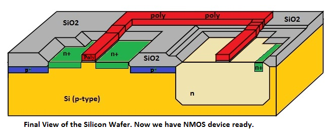
  • In this we are going to create PMOS (Source and Drain) only. We are not creating the NMOS body contact (just because of space issue in the diagram) but the concept remains same as in case of PMOS body contact as we have discussed in the previous post.


Final 3D view of the Silicon Wafer is:


Till now we have created
  • Nwell
  • Active Region
  • Channel Stop Region
  • Field Oxide.
  • Gate Oxide
  • Poly layer.
  • N+ regions (Source and Drain) for NMOS device.
  • P+ regions (Source and Drain) for PMOS device.

In the next post we will talk about adding Metal Contact which will help us to pass the signal or data to MOS devices from the other MOS devices or from the External world.


Monday, November 3, 2014

Implant N+ Impurities: CMOS Processing (Part 4)

Implant N+ Impurities:


Index Chapter1 Chapter2 Chapter3 Chapter4
Digital
Background
Semiconductor Background CMOS
Processing

3.1 3.2 3.3 3.4 3.5 3.6
Fabrication
Steps
Create
N-Well and Field Oxide
Create
Gate Oxide and Poly Layer
Implant
N+ Impurities
Implant
P+ Impurities
Create
Metal Contact

Just to remind you that the complete CMOS fabrication process, we are not discussing in a single post. Complete CMOS fabrication, I have divided into different articles as per above table.

Let’s start with the 3D diagram of silicon wafer where we left in the last post.


Final 2 diagram of last post is little bit small in size for clarifying the further processing. So again I am just expanding that and start the process from there on. :)


Now we will start the process of implant of Phosphorus (N type impurities), to create an N+ region in the P-type substrate. Final outcome of this will be the NMOS devices.

Few things are important here.
  • This is the ideal process. In actual fabrication the Gate Length is affected. I will explain with the diagram later in this post.
  • We are going to add Phosphorus as part of N impurities. We can add other also.
  • As a part of side effect of this process, resistance of poly decreases, Nfet threshold affected. But we are not going to discuss all these in this post.
  • NMOS needs a body contact (which will be of p+ doping) the same as the Source(GND)
  • PMOS needs a body contact (which will be of n+ doping) the same as the Drain (Vdd)
  • From process and steps point of view, there is no difference while creating the NMOS and PMOS devices (except mask and the impurities). So we can interchange the steps (Means First we can create PMOS and then NMOS).

Note:
  • In this post we will create the NMOS (Source and Drain) and PMOS body contact only.
  • Next post will be related to PMOS (Source and Drain) only. We are not creating the NMOS body contact (just because of space issue in the diagram ) but the concept remains same.


As I have mentioned that the channel length will be different, please understand with the help of below diagram. Same concept is going to apply for channel length in case of PMOS devices (which we will not discuss there).


Now the 3D view of the final silicon wafer is:


Till now we have created
  • Nwell
  • Active Region
  • Channel Stop Region
  • Field Oxide.
  • Gate Oxide
  • Poly layer.
  • N+ regions (Source and Drain) for NMOS device.

In the next post we will talk about adding P+ impurities which will help us to create PMOS devices.


Must Read Article

Related Posts Plugin for WordPress, Blogger...